
Cost/benefit considerations
For R&D requirements, the costs are usually understood and allowed for in the sense that the customer has a real choice over the type of test that needs to be done and how best it is realised. However, as all types of measurement are needed in the R&D environment, expensive pieces of test equipment are being used for low cost measurements, which is tying up valuable R&D time.
In a wider context, in addition to R&D customers aiming to derive even tighter performance thresholds, other parallel research work may be required from outside contractors who have little finance available for capital expenditure on test equipment, and who therefore may procure the services of a research organisation or university department to perform the work on their behalf.
Interestingly, many VNA applications require only basic functionality, such as S-parameter measurement capability and some subsequent post-processing software. To date, this combination of features has only been possible by using existing high-performance VNAs: a situation that has led to users being reluctant to pay for unused advanced VNA features: especially in applications where the size of the equipment has presented additional difficulties in terms of the available space and the design of the testing location.
Simplicity and compactness
With the latest developments in lower-cost and more compact VNAs, however, the simplicity and compact nature of the VNA hardware allow it to be quickly prepared for antenna S-parameter measurements (Figures. 1 and 2), as used by Dr Massimo Candotti at the Antenna Measurement Laboratory, Queen Mary University of London.
In this application, the VNA can be mounted vertically against the antenna chamber, allowing it to be as close to the antenna under test as possible. The Anritsu Shockline MS46322A, for example, can be quickly prepared for bench use for standard microwave device and antenna S-parameter measurements or for more dedicated applications. Unlike earlier VNAs, which used GPIB for their commands and could only cope with one frequency measurement per turntable revolution, the Shockline VNA has high directivity and signal/noise ratio in conjunction with high measurement and processing speeds, and therefore allows multiple frequency beam pattern measurements at the same time as the turntable is moving.
Performance of this nature was only previously available in high-end VNAs, which are large and bulky, and have many other features that would not necessarily be used even though they had been paid for.
Automated testing
Another typical application example for the MS46322A is its use in an automated test system with an in-house LabVIEW graphic user interface capable of the simultaneous retrieval of multi-frequency antenna beam pattern measurements while the antenna under test is rotating on the turntable. By taking advantage of the fast measurement sweeps of the MS46322A, even at a low IF bandwidth of 700Hz, a set of beam patterns at up to 11 frequencies per full 360° rotation of the turntable can be recorded with dynamic ranges greater than 60 dB for low gain antennas.
This application reduced the testing time in the EMC chamber dedicated to electrically small antennas (generally PCB antennas for a variety of mobile device applications from 400MHz up to 12GHz), by allowing users to test the two major antenna beam patterns in the E- and H-planes in less than 90 seconds: the time the turntable takes to go to start position, complete the full 360° scan and go back to the antenna boresight position.
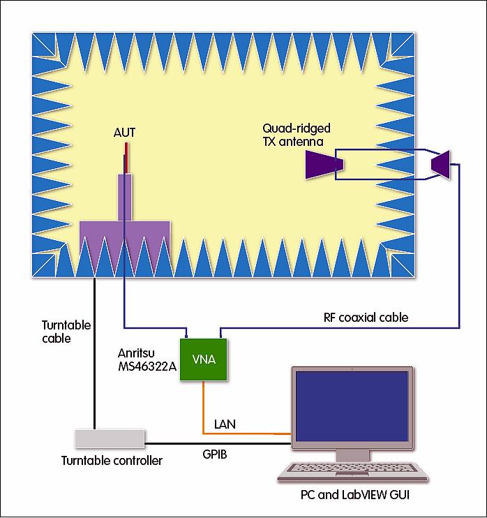 Figure 2. EMC chamber for antenna testing using a VNA-based beam pattern measurement system
As the cost of VNAs falls, applications are being driven more and more by users that are not traditional VNA users – in areas such as materials testing and particle scanning, for example – where the cost of VNAs had previously made it difficult to justify their purchase.
New technologies
Now, however, we are seeing the emergence of low cost VNAs with dynamic ranges of up to 100dB and sweep speeds of less than 100µs/point. This combination of lower cost and high performance is the result of a number of technical developments, including Anritsu’s patented ShockLine ‘VNA on a chip’ architecture using nonlinear transmission-line technology. These nonlinear transmission lines or ‘shock lines’ generate narrow impulses at high frequencies which extend the operating range of the sampling receivers to 40GHz and beyond. With a higher local-oscillator frequency, this sampling technique yields better noise performance than harmonic mixing, especially at higher RF frequencies. Together with the higher third-order intercept point (IP3), this translates directly to an improved dynamic range.
With a single-board RF VNA implementation, and using a COTS power supply and PC, cost is also reduced by eliminating the front panel and keypad, which are not required remote applications such as monitoring, ATE and distance learning. This gives the user the choice and flexibility to add their own interfaces or displays, allowing them to focus on basic features and functions such as S-parameters and/or time-domain testing.
Author profile
Paul Holes is field application engineer for RF and microwave products at Anritsu.


