
Technical tests, combined with ever-shortening time to market and regulatory pressures, has led to a reliance on specialist contract electronics manufacturers (CEMs) to help mitigate risk at the earliest stage of the development process.
The demand for miniaturisation and the physical testing issues it generates, are not unique to communications technology. However, the sheer density of wireless networks and the number of devices needing to connect to them, poses huge challenges when mitigating against issues of signal emissions.
Conservatively, more than 300 types of consumer devices operate in the 2.4GHz band on the radio wave spectrum, making the margins for error on interference incredibly low – especially when all those devices operate within the same room.
The commercial application of highly dynamic radio systems sees this issue multiplied. When you consider that a state-of-the-art automated warehouse can contain anywhere from 1,000 to 2,000 devices operating on a network confined to a signal facility, issues of emissions grow dramatically.
Combine these tough design trails with the massive time-to-market pressures OEMs face and once an OEM’s product reaches the manufacturing stage, designers already need to be working on its next generation if they are to maintain a competitive edge. This means that developers have to increasingly rely on CEMs to help mitigate risk and ensure that products reach the market on time, on budget and fully tested.
CEMs have traditionally been relied upon in the latest stage of the NPI process to assemble products while maximising quality. However, contract manufacturers in the low to medium volume, high technology sector are required to offer far more than simply populating PCBs – they must add value through advising designers on buildability, incorporating testing solutions into early design plans, maximising board real estate, creating rigorous test solutions and improving efficiency throughout the assembly process.
Having that input during initial planning and design phases makes projects much more scalable, while more upfront testing offers the potential for significant cost reduction and greater efficiency throughout the manufacturing process. As the rate of product turnover increases in a competitive marketplace, this involvement becomes crucial for future designs. The lessons from the last device’s assembly will determine the design of the next.
In-house advice
In-house PCB designers will look to advise on everything from smaller changes, such as adding in test pads and points, to more fundamental ones, such as substituting components. With communications systems that advice tends to focus on changing connectors. Many standard types of FSC connectors used in designs are easy to manufacture, but often interfere with rigorous tests, and frequently do not stand up to such testing. In the past we’ve had to design throwaway custom boards that enable us to run all available tests on the individual parts, before re-assembling the boards to the specifications they were designed to.
Today, OEMs can make use of an array of standardised off-the-shelf modular components when designing new communications systems, rather than having to design bespoke Bluetooth or Wi-Fi modules. However, pitfalls still exist should a designer choose to incorporate the wrong component into a product – issues of quality, counterfeit products and traceability and prolonged availability can still pose areas of risk. Consequently, procurement departments have a crucial role to play.
Too frequently the creation of test solutions are mistakenly left until later in the design process, and often lead to very real challenges.The demand for ever smaller devices, places board real estate at a premium, and inevitably results in a reduction in test points. We have actively sought to drive the implementation of package-on-package (POP) solutions in UK manufacturing. The SMT capability to stack components and build up, rather than mounting them side by side on a board creates major efficiencies.
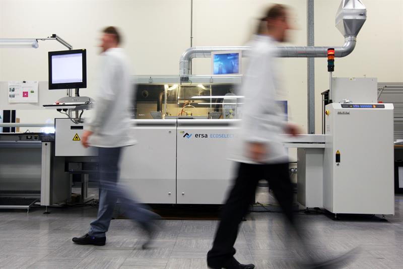
Typically, Axiom, pictured left, build PCBs with POP devices to two stacks and use Fuji SMT Lines for the accurate placement of Micro BGA Devices as well as SMT Parts down as small as 01005. This can throw up issues around pad precision for various parts, which need to be extremely accurate for ensuring correct placement. This is therefore another potential issue that can be mitigated by working with OEMs at the earliest possible stage.
Often, the design of a bespoke test solutions will use a full suite of testing solutions including AOI, Flying Probe, Teradyne, JTAG, Boundary Scan or Functional Tests, depending on what’s needed. In the case of communications hardware, it’s likely that some form of conductive, radiated or screened tests will be required to ensure a device’s emission remains within its designated band. For example, the majority of consumer devices today will remain in the standard 2.4GHz band (used for Wi-Fi, Bluetooth and ZigBee networks), but devices for the medical and industrial sectors will likely seek to exploit the far less crowded 5Ghz spectrum.
Extra step
Following our own testing and diagnostics, we take an extra step to ensure conformation to emission standards, but it’s one we will believe will become increasingly common in the industry. Using specialist EMC & safety test houses, we conduct a pre-compliance run, which provides independent verification that a product meets all EMC requirements, including Radiated, Conducted and Harmonic Emissions, as well as Radiated and Conducted Immunity.
Having been involved throughout the design for manufacture and test process, we can then work with the test house to solve any issues on the spot. At this stage of testing communications systems, one of the most effective ways to reduce emitted and received interference, without complete board re-design, is the addition of Ferrite Cores to external leads. Using testing houses to identify issues and make on-the-spot changes is akin to taking your car in for a quick service before you need to take it in for a full MOT.
Other common tweaks identified at this stage of testing, which can avoid the need for product redesign, include product earthing. Generally, this involves adding earth wires to the chassis throughout testing. While adding cost and effort to the process, it ultimately ensures maximum testing capability.
Another issue that can be thrown up under rigorous specialist testing is that of overheating. Sometimes this side-effect was not envisaged during the design phase, but systems are often designed to run at reasonably high temperatures, and so determining when components on a board are too hot can be challenging. To ensure optimal temperatures, steps taken at this stage can vary from minor board layout adjustments, to the addition of fans to reduce heat.
In order to maximise quality and efficiency throughout the NPI design process, it is crucial that learnings are efficiently translated to the design of the next generation of a product. This facilitates more cohesive procurement strategies, rigorous testing and the development of more creative assembly processes.
Author profile
David Davies is managing director of Axiom Manufacturing Services.


