
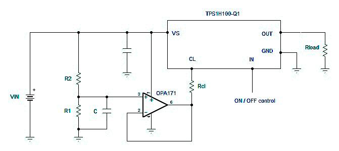
TPS1H100-Q1 load switch
The TPS1H100-Q1 is a single channel, fault-protected load switch, rated at 40V and having a programmable current limit. It is part of a family of automotive single, dual (TPS2H160-Q1) and quad (TPS4H160-Q1) channel devices.
Its current limit accuracy depends on the load current and for the load currents considered here then it is ±20% in temperatures ranging from -40 to +150°C.
Constant power limiter
The current limit function of TPS1H100-Q1 works by sourcing a mirror of the load current (Iout) divided by a constant (Kcl = 2000) out of its CL pin and through the resistor (Rcl) connected to it. When the voltage across Rcl reaches a threshold (Vcl = 1.23V), then it enters current-limit mode according to the re-arranged datasheet equation:
Vcl= (Rcl x Iout)/Kcl
In the constant power limiter application, the input voltage to the load switch (VIN) is scaled by a resistor divider according to a ratio, Div, given by:
Div = R1/(R1+R2)
and buffered by an op-amp in unity gain configuration. Its output is connected to Rcl (Figure 1). The voltage across Rcl now depends on the mirrored load current (Iout / Kcl) through it, plus the voltage set by the scaled VIN. If VIN increases, then the op-amp output voltage increases and this will cause TPS1H100-Q1 to enter current limit at a lower current than before. Therefore the current limit is modulated by VIN and this is an approximate power limit function.
The VIN-modulated current-limit equation is given by:
Vcl = (VIN x Div) + [(Rcl x Iout)/Kcl]
This is a simple approach and the current-limit is proportionally modulated using VIN, whereas a true power limiter would multiply the voltage and current.
For example, if the nominal VIN = 12V(typ) and the max load Iout=0.65A and the input power limit is such that the power is approximately constant for a variation in VIN of ±25%, then the simultaneous equations can be constructed:
1.23V = (VIN1 x Div) + [(Rcl x Iout1)/Kcl]
and
1.23 = (VIN2 X Div) + [(Rcl x Iout2)/Kcl]
Where Iout1 is the load current to give constant power at a VIN1 = 15V (i.e. Iout1 = 0.52A) and Iout2 is the load current to give constant power at a VIN2 = 9V (i.e. Iout2 = 0.87A). Note that Iout is the current through the internal MOSFET of the IC and is the same as the input current. Solving the two equations gives Div ≈ 0.05 and Rcl ≈ 1k8. In Figure 1, a ratio Div = 0.05 is obtained by selecting R1=1k and calculating R2=18k5. A noise filtering capacitor of 10nF across the divider was used.
The actual power limit is a curve with minimum values at 9V and 15V, and rising to a maximum at the 12V mid-point (Figure 2). The equations allow you to calculate and set a minimum power that the circuit will deliver over the required VIN range.
Another question is what maximum current limit will be seen using the technique in the above example. The maximum current limit of 1.37A would occur when the op-amp output is 0V, but in practice this is not reached because TPS1H100-Q1 has an Undervoltage Lockout (UVLO) of 3.5V and below that voltage it is held off.
In the example, the minimum op-amp output will be 3.5Div = 0.18V. Therefore, the max current limit Iout(max) is given by:
Iout(max) = (Kcl/Rcl)(1.23 - 0.18)
OPA171 was used in the tests that follow, as it is able to sink the Iout/Kcl current at ~0V output and having a common-mode input range that includes 0V. It is available as an automotive-grade device: OPA171-Q1.
TPS1H100-Q1 has a Current-Sense or a Status output that enables a host microcontroller to detect the onset of current limit and start a counter. After the counter has expired, the IC could enter a hiccup mode, whereby it is disabled for a period of time before being re-enabled. The IC also has thermal limit protection.
Results
The circuit was simulated using TINA-TI with an overload of 2.2Ω and VIN was ramped over a range from 1.5 to 20V over 15ms. A 2.2Ω load is a severe overload which means the IC is in power-limit mode over the full range of VIN (Figure 2). Due to its UVLO, the IC only becomes active at VIN ≥ 3.5V. The op-amp output voltage ramps with it and the current-limit changes as shown by the falling IOUT. Over the appropriate VIN range from 9 to 15V, then the power at 9V and at 15V is the minimum value of 7.8W rising to 8.3W at VS=12V. In other words, for a 50% change in VIN, the power limit changes by only 6%.
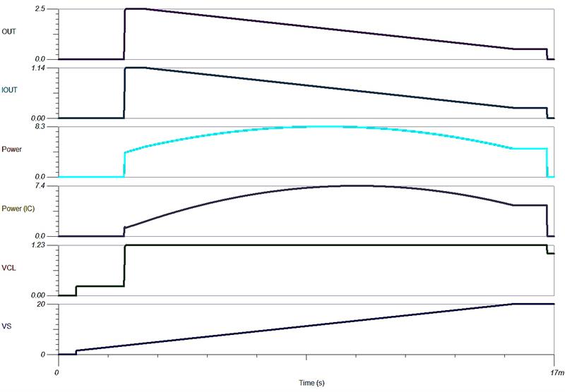 Figure 2 – Simulation results for Rload = 2.2Ω. OUT and IOUT are the output voltage and current from the load switch, power is computed as VS x IOUT, power(IC) is the power dissipated in the IC computed as (VS-OUT) x IOUT, VCL is the voltage on the current-limit CL pin and VS is the input voltage VIN
Moderate overload such as 10Ω gives normal operation until VIN is greater than 9V, at which point maximum power is reached and the circuit power-limits thereafter (Figure 3).
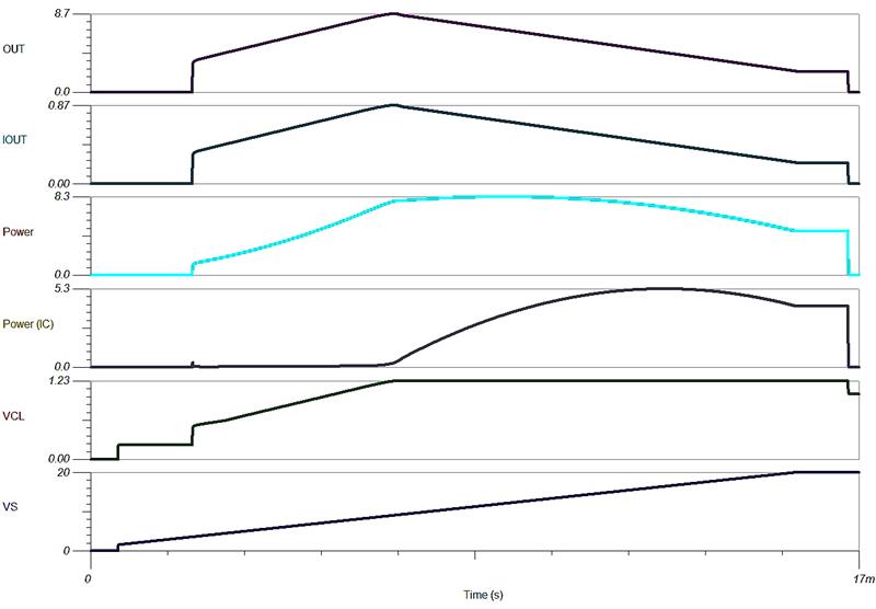 Figure 3 – Simulation results for Rload = 10Ω. OUT and IOUT are the output voltage and current from the load switch, power is the input power, power(IC) is the power dissipated in the IC computed as (VS-OUT) x IOUT, VCL is the voltage on the CL pin and VS is the input voltage VIN
The circuit of Figure 1 was bench tested under the conditions of VIN being manually varied in steps, from 4 to 20V with a moderate overload of 10Ω applied. The power is controlled to be constant at 7.8W rising to 8.5W over a range of VIN from 8.7 to 17V (Figure 4).
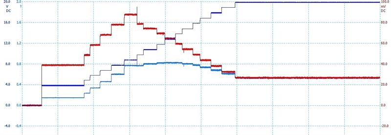
A severe overload of 2.2Ω was applied and VIN varied as before. Figure 5 shows the bench test result. The power reaches a max of 9W and is greater than 8W from 9 to 16V. Under these overload conditions, the high power is dissipated in the IC itself and thermal limit protection is applied after the die reaches the maximum temperature. The thermal limit periodically turns the IC off/on as the IC heats up and cools down.
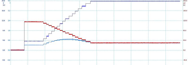 Figure 5 - Test results with 2.2Ω Load. VIN (dark blue, 4V/div), OUT current (red, 100mV=1A, 400mA/div) and power (light blue, 0.1V=1W, 8W/div). Timebase = 1sec/div.
As a further example, startup into a 1000µF load in parallel with 120Ω is shown in Figure 6. An uncharged capacitor is a virtual short circuit and the IC limits the current, plus the op-amp circuit limits the power to 8W. VOUT is not shown but ramps to 12V during the main current/power pulse in Figure 6. After charging, the current/power drops back down to the 120Ω load.
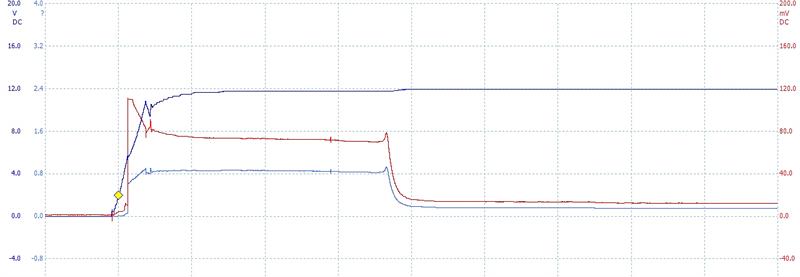 Figure 6 – Test results -start-up into a 1000µF // 120Ω load. VIN (dark blue, 4V/div), IN current (red, 100mV = 1A, 400mA/div), power (light blue 0.1V=1W, 8W/div). Timebase = 5ms/div.
Conclusion
The technique described provides an approximate power limit over a range of VIN.
Author profile
Dan Tooth is senior field applications engineer at Texas Instruments.


