
But there was general acceptance that, one day, Moore’s Law would slow as the Laws of Physics came into play. Questions are now asked about how much longer silicon processes can be scaled and, importantly, their cost.
However, one company is working on ways to alleviate the problems of scaling silicon processes, rather than overcome them. Scott Bibaud is CEO of Atomera, previously known as Mears Technologies. “The latest nodes are too expensive,” he said, “and I can see the point beyond which we can’t progress. Industry has known about this for a while and is struggling to create solutions.”
Dr Robert Mears set up his company in 2001, with the idea of applying atomic level material science to the problem. He developed Mears Silicon Technology (MST) as a way to improve the performance and power efficiency of devices, while potentially reducing their cost.
Bibaud added: “When I saw what Robert was develop, I saw a near term solution to some of the industry’s problems.”
So what is MST? “It’s a thin film which is applied to silicon wafers,” Bibaud explained. “It can be integrated into existing processes, where it could make chips run more quickly, with better power consumption and increased yield.
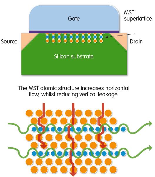
Figure 1: MST is said to bring improved efficiency, better performance and lower power consumption to a range of chips
“Essentially,” he continued, “you can add it to any process technology, but the benefit you obtain is similar to that which derives from a process shrink. So a device made on a 28nm process, for example, would perform like a 20nm device. It’s also useful to upgrade devices; for example, some chips that might not be able to shrink beyond a 28nm process.”
This, Bibaud contends, should make MST attractive to anyone building semiconductors. “Leading edge processes are now costing more than $1billion to develop. Using our technology, you can improve an existing process for somewhere in the tens of millions of dollars.”
Dr Mears explained the approach. “A lot of processes use silicon epitaxy; it’s been used for years in analogue electronics. Intel introduced compressive strain for PMOS and, since then, epitaxy has been accepted in the CMOS world.”
The concept of MST is that, at various points, you stop the growth of silicon and insert, according to Dr Mears, ‘a puff of oxygen’. “Then you continue with the process,” he said. “And you can use other elements. Overall, it’s about growing crystalline silicon, but it’s crystalline silicon with a twist.”
| “MST could enable a next generation [chip] with higher performance, lower power consumption and better yield.” | “Overall, it’s about growing crystalline silicon, but it’s crystalline silicon with a twist.” |
According to Atomera, MST is an ultra thin film of reengineered semiconductor that incorporates layers of non semiconductor material. For CMOS applications, partial monolayers of oxygen are typically deposited during epitaxy of a thin single crystal silicon layer. This layer may be only a few tens of lattice spacings thick. The engineered silicon lattice can than offer particular electrical properties which, the company claims, address key device engineering challenges associated with cost reduction and lower power consumption.
“It enhances mobility for PMOS and NMOS using a single film,” Dr Mears asserted.
On its website, Atomera contends that MST enables increased carrier mobility and drive current and says these benefits can be obtained with devices such as microprocessors, logic, memories, analogue and power management. It asserts that drive and effective current increases of 10 to 20% have been demonstrated, as well as improved mobility at high and low fields.
Dr Mears said that, in the early days of MST, he set about developing a blanket wafer approach. “One of the things we were aware of was the issue of heat; too hot, and you vaporise the oxygen. But if you can put it into the process in the right way, it’s stable.”
According to Dr Mears, the MST film adds confinement and assists with the overall quantum mechanical confinement of the carriers. “There is also more energy separation in the sub bands,” he argued, “with less scattering and therefore higher mobility.”
Dr Mears said there is also interaction with electrical dopants. “The MST film is like a ‘band aid’, stopping the upward diffusion of dopants. That means you can have a profile that’s within the depletion region, but which fills rapidly at the surface conduction region.”
The MST process is said to be applicable across a number of technologies. “It works with analogue and with 180nm processes,” Dr Mears noted, “and we are doing early simulation work with FinFETs. Even analogue nodes can benefit through the reduction of short channel effects.”
Typically, Atomera expects the MST process to be applied at the 130nm node and smaller. “Typically, at these nodes,” Dr Mears explained, “you have to use ‘halo doping’.” In this process, the amount of dopants is higher near the source and drain. “This impairs analogue performance, resulting in worse matching and more noise. Using MST, the level of halo doping can be reduced and the analogue characteristics recovered.”
However, Dr Mears realised his blanket wafer approach wouldn’t work with all technologies, so he developed a selective process. “Shallow trench oxides can grow the film on exposed areas, through defining where the transistors are. You can then grow the MST layer before the gate. The film is 10nm or so thick, but it improves mobility, variability and matching.”
Early work with Berkeley University on FinFETs at 7nm, said Dr Mears, showed that Vdd could be less than 0.5V and this could enable silicon to be used to at least the 5nm node.
Bibaud sees three main areas of application for MST. “Legacy nodes will be important,” he said, “particularly more than 90nm. These are mainly used for analogue and power devices and it will be important if they can use less power.
“But the biggest opportunity is in the mainstream. Most wafers in production today are using processes between 28 and 65nm. A lot of these chips have a certain amount of functionality, but can’t be shrunk further because they are pad limited. So a lot of high volume chips are stunted because there’s no way to shrink them. MST could enable a next generation version with higher performance, lower power consumption and better yield.
“And there’s FinFETs, where MST can provide foundries with the ability to use bulk silicon and get high yielding devices.”
Although Dr Mears has worked on MST since 2001, the technology has yet to hit the mainstream. “But we have three customers getting close to commercialisation,” Bibaud asserted.
Despite MST appearing to be ‘just another process step’, Bibaud pointed out that every company makes chips differently and, should they select MST, it would have to be ‘tuned’ for each application. “Once they decide to try MST,” he concluded, “they can run wafers and we can optimise our technology for their process.”


