
As a result the power amplifiers (PAs) for these highly distributed small cells need to be able to meet different design criteria to those for macrocells. They have to be able to handle less power (perhaps 60W peak for a 5W cell), because they transmit over shorter distances than macrocells and they need to be engineered for high efficiency, to keep operating costs down, reliability up, and to enable small, light and low-cost enclosures.
One way to meet these design criteria is to use multi-stage LDMOS MMICs, produced using high-volume silicon manufacturing processes. These devices offer high gain, integrated input and inter-stage matching, and so fit the need for small and low-cost PAs, but, due to their use of integrated passive elements, have tended to suffer from relatively low efficiency compared with alternatives.
One solution, developed by Ampleon, is a semi-integrated three-way 1:2:1 PA architecture that is both small and efficient. It has been successfully used to build a 60W MMIC that operates at 2.14GHz with a gain of 27.4dB and an average power-added efficiency (PAE) of 48.5% at 8dB output back-off. The circuit is 35×35mm2 and, as far as we know, is currently offering the best performance at this frequency and power level for a multi-stage MMIC.
Doherty architecture analysed
This is a basic schematic of a PA built using a three-way Doherty architecture.
One important characteristic of a PA is its efficiency when operating at less than its peak power, which is known as ‘back-off’.
Compact design equations can be used to locate the back-off efficiency peaks 1 and 2, of a DPA as below, where 1 and 2 represent the power capabilities of the peak 1 and peak 2 devices normalised to the main device power capability. The back-off efficiency peaks can then be expressed as:
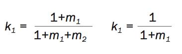
The load modulation of the main device m can then be expressed as:
This gives high-efficiency points located at -2.50dB ( 1 = 0.75) and -9.54dB ( 2 = 0.33), with m = 2.25 for the (1:2:1) power ratio.
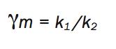
It is possible to simulate the voltage and current profiles of the PA by assuming that its transistors behave as ideal current sources with zero on-state voltage and constant forward trans-conductance, a maximum current limit and a 1V supply. We assume the transistors operate in class-B mode and that all harmonic impedances at the current source are short-circuited.
The equations above, and the simulations shown in Figure 2, say that from an efficiency point of view, the three-way 1:2:1 DPA is better than the 1:2 asymmetric DPA currently used in base stations. The 1:2:1 DPA keeps its efficiency above 67% up to the saturation point, while the efficiency of the 1:2 DPA can dip to 59% before peaking again up to saturation. This means that the 1:2:1 DPA should achieve an average efficiency 6% points higher than that of the 1:2 DPA in the desired 8 to 9dB back-off region.
That’s the theory. What happens in reality? We can calculate the practical power modulation mod of the main device, knowing that m is 2.25 for the 1:2:1 DPA and 3 for the 1:2 DPA. With real devices, which don’t have zero On resistance and zero output RF losses, the actual power modulation of the three-way DPA is lower than theory suggests. This gives us a practical back-off efficiency point real of the 1:2 DPA at -7.8 dB ( real = 0.41). Using a real mod of 1.58 instead of a theoretical 2.25, the practical second back-off efficiency point 2real of the 1:2:1 DPA is located at -8dB.
These calculations show that the efficiency advantage of the 1:2:1 DPA is maintained, and even slightly reinforced, thanks to its extra efficiency peak when operating in back-off. This gives a better average efficiency in the 8 to 9dB back-off region.
A good PA also needs good linearity. One challenge with the 1:2:1 DPA architecture to date has been to build effective practical implementations using passive input splitters. The problem is that, for best efficiency, the current to the main device has to remain saturated and constant from the first back-up point 1 at -6 dB up to the full power condition. This can cause a disruption of the main amplifier load when peak1 reaches voltage saturation at 1. This in turn creates linearity problems that have been experienced demanding modulation schemes such as that used in GSM Multi-Carrier, which need better than -60dBc intermodulation performance.
One way around this is to use independent drive profiling of each amplifier, but this complicates practical implementations so much as to make the approach unaffordable for most base stations.
| Figure 2: Simulated fundamental characteristics of the 3-way DPA |
Practical implementation
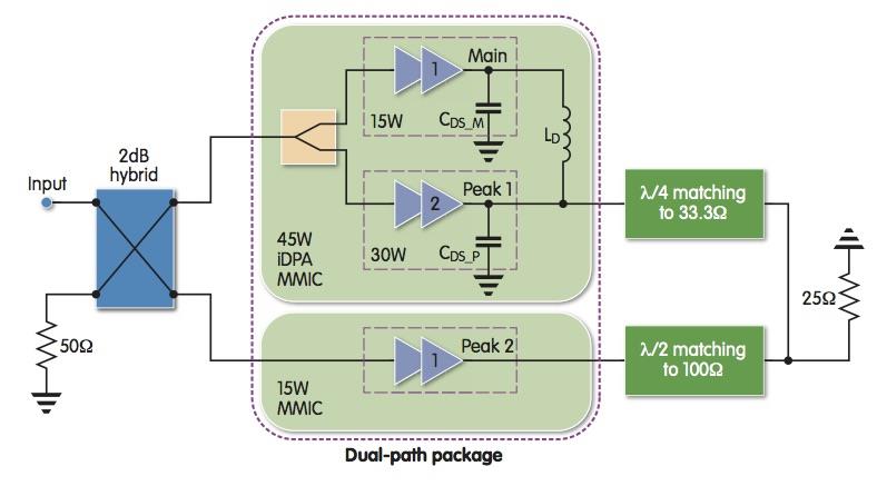
Our integrated Doherty (iDPA) implementation replaces the usual Doherty impedance inverter with a π network formed by the drain-to-source parasitic capacitors (CDS_M and CDS_P) of the main and peak transistors, and a series inductor LD connected between them.
We used this approach to build a three-way 1:2:1 DPA by combining using a dual-amplifier device and a single amplifier device in a dual-path package (see Figures 3), to keep the overall size down.
| Figure 3: Comparing the gain and PAE of the 1:2:1 and 1:2 DPAs |
The three-way DPA was built on an industry-standard PCB of 20 mil height and 3.5 dielectric constant.
Figure 3 compares the gain and PAE for the 1:2:1 and 1:2 DPA architectures. The 1:2:1 amplifier achieves a maximum gain of 27.4dB at 2.14GHz and an average PAE of 47.5% at 8dB back-off, when measured using a 20MHz-wide LTE signal with a peak to average ratio of 7.2dB.
The three-way DPA can be linearized at this power level to achieve a -58dBc adjacent channel power ratio, using digital pre-distortion. Comparing the performance of the 1:2:1 DPA implementation with the standalone performance of the 45W 1:2 iDPA MMIC that forms a part of the three-way architecture shows that the three-way configuration offers an improvement in PAE of 3.5% points, at the expense of 2dB gain.
In conclusion this semi-integrated three-way 1:2:1 Doherty architecture integrates a dual-path device with another amplifier in a small package, and achieves class-leading performance in doing so. This shows that DPA MMICs can be used to build efficient, cost-effective small-cell base stations.
| Author profile Xavier Moronva is senior principal RF engineer with Ampleo |


