
Rumours of the death of Moore’s Law have, so far, been somewhat exaggerated. But there is going to be a point at which in the process of scaling planar structures you simply run out of enough atoms to create viable semiconductor interfaces.
When the inevitable happens, the only option is to follow in the footsteps of NAND flash and start stacking.
The December 2019 International Electron Device Meeting (IEDM), demonstrated the various ways in which chipmakers are thinking about taking that direction. Multichip 3D is already with us thanks to improvements in packaging. But that form of packaging does not have the manufacturing efficiency that has kept Moore’s Law on track so far. That needs monolithic integration and a means to stack transistors on top of each other on the same base wafer.
It’s possible to see the beginnings of a trend towards 3D as a means to improve density in the shift to finFETs over a decade ago. You can easily boost the drive strength of a single transistor simply by adding fins rather than physically widening the device, just as long as you can make the fin pitch tight enough.
This has boosted the effective density of the standard-cell libraries used to design SoCs and demonstrated by a steady reduction in average height of cells, usually measured in terms of the metal tracks used for routing. Where ten- or twelvetrack cell libraries were common in the past, advanced processes are now using between seven and nine. And the chipmakers and EDA-tools suppliers are looking to even fewer.
With finFETs, the process can only go so far. Each fin still takes up horizontal space and that is hitting the limit. So, the next step is to stack the fins on top of each other using so-called nanowires or nanosheets. Imec sees even more potential for cutting out horizontal space by moving to the “forksheet”. This stacks complementary n- and p-doped sheets next to each other, built out of a common pillar. With that you have a full CMOS inverter built into single transistor structure, albeit one that is wider than a single nanosheet device. The overall saving is about 30 per cent, Imec claims, with a track height of five for a workable cell library. But the research institute’s people think three is possible.
The CFET
The previous year at the VLSI Symposia in Hawaii, Imec described another way of building a compact CMOS inverter structure in the space of a single transistor. This was the CFET, a structure that stacks an n-channel device right on top of its complementary p-channel partner. Although it boosts horizontal density even further it leaves the designer with a problem: how to get power in and out as well as logic signals. Rather than take up valuable space and interfere with signal lines, much of the power can go underneath using buried vias. The coarse power grid still takes up routing above the base layer but by diverting much of the local power interconnect underneath, Imec expects to be able to achieve signifi cant and practical layout-density improvements and may not have to wait for the CFET to become a reality to implement the idea.
Stacking could go further though there are practical diffi culties that may prove difficult to overcome.
CEA-Leti has pushed ahead on developing processes that make it possible to put one complete layer of connected transistors on top of another, using reasonably conventional deposition techniques. There is a catch with this approach. Every process has a thermal budget and transistors need high temperatures to heal their crystalline structures after bombardment during the doping steps. With only one base layer of transistors, it is easy to account for that. Doing the same to a second layer risks damaging the interconnect needed to wire up the first layer as well as the devices themselves.
Annealing using high-energy lasers limits the damage though it is slower and more expensive than just baking the wafers in an oven. Even with that more precise form of annealing, it may not be possible to create a second layer with the same performance as the first. This may not matter in practical situations. CEA-Leti has pointed to applications such as artificial intelligence that, with the right architecture, can use slower transistors.
Analogue circuits might also go into the upper layer. Some teams at IEDM late last year looked at taking that idea further and moving the transistors even further up into the metal stack. The ability to even countenance structures with ten or more layers of metal dates back well before finFETs to the early 1990s when chemicalmechanical polishing (CMP) fi rst appeared. Up to that point, three layers of metal were the limit of production techniques.
The cross-sections showed why: the transistors formed hillocks above them that were amplified by each successive layer of routing. Beyond three, it was impossible to create reliable connections. CMP changed that by making it possible to flatten each surface before the next layer went on. If the materials are up to the job, CMP creates planar substrates suitable for making transistors and memory devices.
2019’s IEDM demonstrated the options are expanding. Working with researchers from UC Berkeley, TSMC engineers developed a form of finFET that can be fabricated, again with the help of laser annealing, in between regular metal layers high up in the stack, above those used to route logic signals. These finFETs are much larger than their base-layer cousins and use multiple fi ns to reduce resistance so that they can form the basis of voltage-regulator circuits.
With this type of design, it becomes possible to create very fine-grained voltage control to drive cores at specific speeds to save energy. Another team from TSMC used a similar approach to create SRAM arrays in the metal stack.
Below: The Intel layer-transfer process
Alternative materials
Rather that stick with conventional silicon-based materials, researchers at the Japan-based Semiconductor Energy Laboratory opted for materials that have been proposed for integrating electronics into flat-screen displays: these have the advantage of using near room-temperature processes though they do not produce fast-switching transistors.
They used a combination of oxides based on indium, gallium and zinc to create a flash memory based on a transistor with a gate length of 72nm. Like TSMC’s SRAM, it cannot compete on density with base-layer devices because of the coarse nature of upperlayer metal but the team claimed it could offer better retention times for IoT sensors and can be stacked over multiple layers.
Another option is the graphenelike material molybdenum disulphide – commonly used as an industrial lubricant today – which some believe might ultimately replace silicon entirely. A couple of years ago, TSMC explored it as an option for transistors in the metal stack because like the oxide-based semiconductors it does not need high-temperature processing.
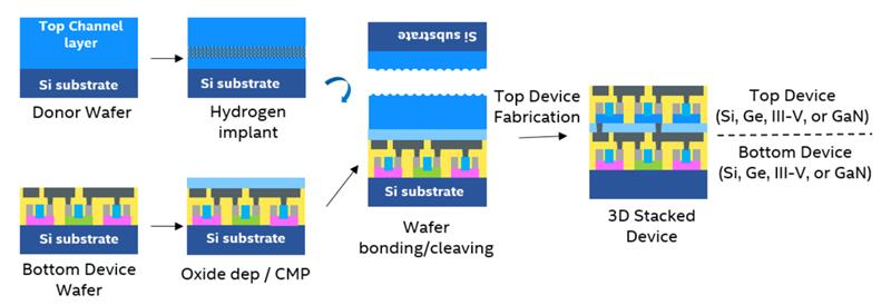
CMP enables another way to approach 3D integration: layer transfer. IBM first proposed this idea in 2003 as a way of mixing crystal orientations on the same wafer. Typically, mobility in p-channel devices is better on a lattice that is rotated with respect to the one favoured for n-channel. One of Intel’s demonstrations last year used germanium in the channel of the PMOS devices formed on a wafer that is polished down and placed on a receiving layer that holds the silicon n-NMOS devices before the donor wafer’s substrate is cleaved away and again polished smooth. The second demonstrator opted had gallium nitride in the NMOS layer, to support RF circuits running at up to 7GHz.
Layer transfer is unlikely to be the cheapest option because of the need for multiple wafers. However, raw polished wafers are cheap compared to the processes that put devices onto them.
Where performance demands balanced CMOS performance, layer transfer may be the best option.
But for integration density, monolithic processes that implement unbalanced devices may prove to be the best mass-market alternative to 3DIC stacking – and the approach that extends Moore’s Law bey