
Ever since the advent of the monolithic silicon-based A/D converter, these devices have been keeping pace with the rapid advancements in silicon processing technology.
Over the years, silicon processing technology has advanced to the point where it is now possible to design economically A/D converters which feature powerful digital processing capabilities. While earlier generations of A/D converters featured very little digital circuitry outside of error correction and digital drivers, today’s gigasample per second converters – also known as RF sampling A/D converters – are made using sophisticated 65nm CMOS technology, allowing them to pack a lot more digital processing power in order to enhance device performance.
With sample rates in the Gsample/s realm, there is also a huge payload of data. Take the AD9680, a dual 14bit JESD204B compatible A/D converter as an example. At its maximum sample rate of 1.25Gsample/s, the converter streams:
14bit x 2 converter channels x 1.25Gbit/s = 35Gbit/s
Extracting this amount of digital data will require an enormous number of LVDS routing lanes. The JESD204B standard was adopted in order to facilitate the implementation of this large data throughput. JESD204B is a high speed, data transmission protocol that employs 8b/10b encoding and scrambling, amongst other features, and at providing adequate signal integrity. Using the JESD204B standard, the total throughput now becomes:
16bit x 2 converter channels x (10/8) x 1.25Gbit/s = 50Gbit/s
The JESD204B standard allows the data throughput to be split across four high speed serial lanes, each carrying 12.5Gbit/s. If you compare this to an LVDS interface where lane rate may be capped at about 1Gbit/s, the chip would need more than 28 pairs!
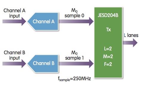
| Figure 1: Setting up the AD9250 |
A quick inspection of the AD9680’s data sheet reveals there is quite a bit of ‘alphabet soup’ as far as setting up the link goes. Whereas earlier generation LVDS A/D converters were easier to implement, the more recent JESD204B based A/D converters are a bit more complicated. And this becomes even more complicated when you take into account the internal digital down converter (DDC) set ups.
A/D converter set up is determined primarily by three letters:
- L; the number of lanes per JESD204B link
- M; the number of converters per JESD204B link
- F; the number of octets per frame of data in the JESD204B link
Let’s take the AD9250 – a dual 14bit, 250Msample/s JESD204B A/D converter – as an example. Figure 1 shows the block diagram of the AD9250 in its default set up. In this set up, the JESD204B link is pretty straightforward, as there is no additional digital processing undertaken. In the JESD204B link, Channel A becomes Converter 0 (M0) and Channel B becomes Converter 1 (M1), which means the value of M becomes 2. The total line rate for this setup is:
[M x N’ x (10/8) x fout] / L = [2 x 16 x 1.25 x 250M]/2 = 5Gbit/s
Compare this to the AD9680 sampling at 1Gsample/s, but with two digital down converters in a complex (I/Q) set up. Figure 2 shows the AD9680’s set up when the DDCs are used to reduce the data sampled at 1Gsample/s by a factor of four. This results in an output sample rate (FOUT) of 250Msample/s.
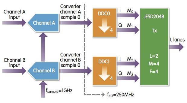
| Figure 2: Setting up the AD9860 with two DDCs set to decimate by four |
It is clear from Figure 2 that the AD9680 can effectively reduce the sample rate using the internal on-chip DDCs. Since each DDC outputs a 16bit stream, the actual (physical) converter bit streams are now decoupled from the ‘M’ parameter of the JESD204B alphabet soup. As per the standard, M is the number of converters per link. In the modified scenario, M now becomes a parameter called a virtual converter. Even though the AD9680 only has two physical A/D converter channels (A and B), when the DDCs are enabled in complex output mode, there are now four different 16bit data streams passing to the JESD204B interface, which ‘sees’ four (virtual) converters sending bit streams.
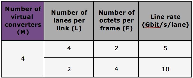
| Table 1: Available options for the JESD204B interface in the AD9680 |
The output line rate in this case becomes:
[M x N’ x (10/8) x fout]/L = [4 x 16 x 1.25 x 250M]/2 = 10Gbit/s/lane
The flexibility of the AD9680’s JESD204B interface becomes apparent here, as there are now two options available, depending on the line rate accepted by the receive logic (ASIC or FPGA). Table 1 shows the available options for the JESD204B interface in the AD9680 setup shown in Figure 2. Table 2 shows the virtual converter mapping available for a dual-channel A/D converter like the AD9680 with four DDCs.
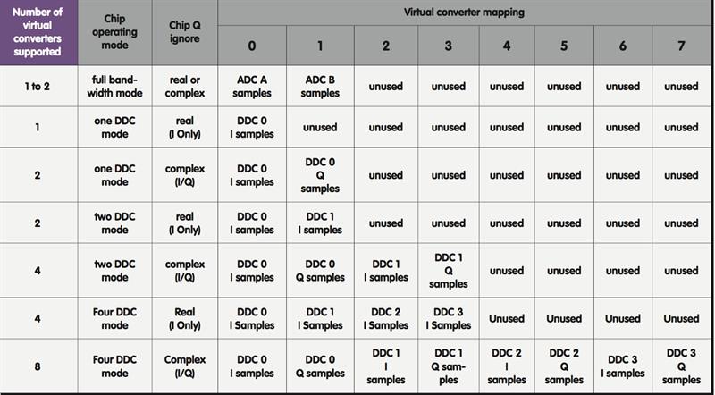
| Table 2: Virtual converter mapping options for the AD9680 |


