One of the largest opportunities for IoT applications is environmental sensing. At the simplest, these could be measuring temperature, but more complex devices are being considered which can assess environmental quality. However, not only do such sensors need to be low cost, some may even be disposable. Enabling this vision will need new manufacturing approaches. And a team from Georgia Tech in the US believes it might have made significant progress in that direction.
According to the researchers, they have developed a technique by which GaN based gas sensors can be grown on sapphire substrates and then transferred to metallic or flexible polymer support materials. The technique, says the team, could enable the production of low-cost wearable, mobile and disposable sensing devices for a wide range of environmental applications. Transferring the GaN sensors to metallic foils and flexible polymers is said to doubles their sensitivity to nitrogen dioxide gas and to boost response time by a factor of six.
Sensors produced using the Gatech process are said to be capable of detecting ammonia at parts-per-billion levels and to differentiate between various nitrogen-containing gases.
The technique is based on growing thin sacrificial layers of boron nitride on a sapphire substrate using metal organic vapour phase epitaxy (MOVPE).
“Mechanically, we just peel the devices off the substrate, like peeling the layers of an onion,” explained Professor Abdallah Ougazzaden, director of Georgia Tech Lorraine. “We can put the layer on another support that could be flexible, metallic or plastic. This technique opens up a lot of opportunity for new functionality, new devices – and commercialising them.”
The process begins by growing monolayers of boron nitride on 2in sapphire wafers using MOVPE at approximately 1300°C. The boron nitride surface coating, which is only a few nanometres thick, produces crystalline structures that have strong planar surface connections, but weak vertical connections.
“Not only can we differentiate between these gases, but because the sensor is very small, we can detect them all at the same time with an array of sensors.” |
Aluminium gallium nitride (AlGaN/GaN) devices are then grown on top of the monolayers at a temperature of about 1100°C, also using MOVPE. Because of boron nitride’s crystalline properties, the devices are only attached weakly to the substrate and can be ‘peeled off’ and transferred to other substrates without inducing cracks or other defects. The sapphire wafers, meanwhile, can be reused to grow new sensors.
According to the team, this approach for engineering GaN-based sensors is a key step towards economically viable, flexible sensors with improved performances that could be integrated into wearable applications.
So far, the researchers have transferred the sensors to copper and aluminium foil and to polymeric materials. In operation, the devices can differentiate between nitrogen oxide, nitrogen dioxide and ammonia. Because the devices are approximately 100 x 100µm, sensors for multiple gases can be produced on a single integrated device.
“Not only can we differentiate between these gases, but because the sensor is very small, we can detect them all at the same time with an array of sensors,” said Prof Ougazzaden, who expects the devices could be modified to detect ozone, carbon dioxide and other gases.
The GaN sensors could have a range of applications from industry to vehicle engines – and for wearable sensing devices. The devices are attractive because of their advantageous materials properties, which include high thermal and chemical stability.
“The devices are small and flexible, which will allow us to put them onto many different types of support,” said Prof Ougazzaden . “Not only can we have flexibility in the substrate, but we can also improve the performance of the devices just by moving them to a different support with appropriate properties. “The properties of the substrate alone make the difference in the performance.”
In future work, the researchers hope to boost the quality of the devices and demonstrate other sensing applications. “One of the challenges ahead is to improve the quality of the materials so we can extend this to other applications that are very sensitive to the substrates, such as high-performance electronics,” Prof Ougazzaden concluded.
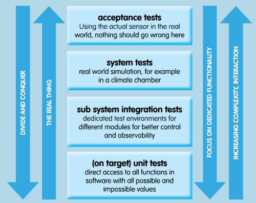
| ams develops a Software Quality Requirements Standard to avoid sensor software risk A digital sensor is no longer a simple component, like its analogue forerunner, because it runs embedded software – and software introduces risk, writes Stephan Puri-Jobi. While system designers can have a high level of confidence in the expected performance of a sensor’s hardware under known operating conditions, how can they be as confident in a sensor’s embedded software? Almost every digital sensor consists of: an analogue front end; driver code; algorithms; and glue logic. This means every digital sensor includes different software components with different requirements. Testing algorithm code is straightforward – for a given set of input values, the tester knows exactly what output to expect. And since this section of code does not need to know where the data is coming from, it is not dependent on the sensor hardware. By contrast, testing driver code requires simulation of the hardware. The system’s sequencing also needs to be verified. For instance, the initialisation and calculation routines might be verified independently, but they must be called in the right order. Finally, the operation of the software must be verified in unusual conditions. How can the user estimate the probability of a sensor IC’s failure due to a software bug? In automotive electronics, ISO 26262 provides a framework for predicting the failure rate of a system in its intended application. But, while ISO 26262-style validation is usually inappropriate for consumer products, their manufacturers need to have high confidence in the quality and reliability of the sensor ICs they use. To give customers a way to estimate the level of confidence in sensor software, ams has developed a Software Quality Requirements standard (see diagram). This defines software quality levels and requirements for all ams software projects, laying down a standard development and testing process.
In this way, ams can show the software embedded in a digital sensor IC can provide robust, predictable performance. Author profile: |